


Optical detectors are essential components in various industries, including telecommunications, medical imaging, and environmental monitoring. These devices convert light signals into electrical signals, allowing for the detection and analysis of light in a wide range of applications. As technology continues to advance, the manufacturing processes for optical detectors have also evolved to meet the increasing demand for high-performance and cost-effective devices.
Another emerging manufacturing process for optical detectors is the use of nanomaterials such as quantum dots and nanowires. These materials have unique optical properties that can enhance the sensitivity and efficiency of photodetectors. In the case of quantum dot detectors, the manufacturing process involves synthesizing nanocrystals of semiconductor materials and incorporating them into the detector structure. This allows for the detection of a wider range of wavelengths and improved signal-to-noise ratios.
In addition to semiconductor materials and nanomaterials, 3D printing technology is also being used in the manufacturing of optical detectors. 3D printing allows for the rapid prototyping and production of complex detector designs, enabling manufacturers to quickly iterate and optimize their devices. This technology is particularly useful for customizing detectors for specific applications or creating novel detector geometries that are not possible with traditional manufacturing methods.
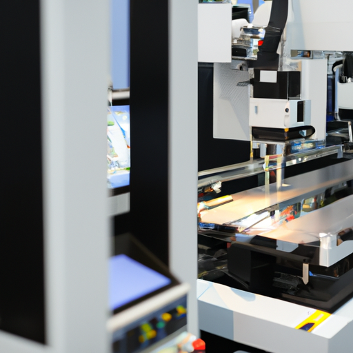
Furthermore, advancements in microfabrication techniques have enabled the production of miniaturized optical detectors with high performance and low power consumption. Microfabrication processes such as photolithography and etching allow for the precise patterning of detector structures on a micron scale. This results in compact and lightweight detectors that can be integrated into portable devices or embedded into larger systems.
Moreover, the integration of artificial intelligence and machine learning algorithms in the manufacturing process has also improved the efficiency and quality of optical detectors. These technologies can analyze large datasets to optimize the design and fabrication parameters of detectors, leading to faster production times and higher yields. Additionally, AI algorithms can be used to automate quality control processes and detect defects in detectors, ensuring that only high-quality devices are shipped to customers.
Overall, the latest manufacturing processes for optical detectors are focused on improving performance, reducing costs, and increasing production efficiency. By leveraging semiconductor materials, nanomaterials, 3D printing, microfabrication techniques, and artificial intelligence, manufacturers can create advanced detectors that meet the demands of modern applications. As technology continues to evolve, we can expect to see further innovations in the manufacturing of optical detectors, leading to even more sophisticated and versatile devices in the future.
Optical detectors are essential components in various industries, including telecommunications, medical imaging, and environmental monitoring. These devices convert light signals into electrical signals, allowing for the detection and analysis of light in a wide range of applications. As technology continues to advance, the manufacturing processes for optical detectors have also evolved to meet the increasing demand for high-performance and cost-effective devices.
Another emerging manufacturing process for optical detectors is the use of nanomaterials such as quantum dots and nanowires. These materials have unique optical properties that can enhance the sensitivity and efficiency of photodetectors. In the case of quantum dot detectors, the manufacturing process involves synthesizing nanocrystals of semiconductor materials and incorporating them into the detector structure. This allows for the detection of a wider range of wavelengths and improved signal-to-noise ratios.
In addition to semiconductor materials and nanomaterials, 3D printing technology is also being used in the manufacturing of optical detectors. 3D printing allows for the rapid prototyping and production of complex detector designs, enabling manufacturers to quickly iterate and optimize their devices. This technology is particularly useful for customizing detectors for specific applications or creating novel detector geometries that are not possible with traditional manufacturing methods.
Furthermore, advancements in microfabrication techniques have enabled the production of miniaturized optical detectors with high performance and low power consumption. Microfabrication processes such as photolithography and etching allow for the precise patterning of detector structures on a micron scale. This results in compact and lightweight detectors that can be integrated into portable devices or embedded into larger systems.
Moreover, the integration of artificial intelligence and machine learning algorithms in the manufacturing process has also improved the efficiency and quality of optical detectors. These technologies can analyze large datasets to optimize the design and fabrication parameters of detectors, leading to faster production times and higher yields. Additionally, AI algorithms can be used to automate quality control processes and detect defects in detectors, ensuring that only high-quality devices are shipped to customers.
Overall, the latest manufacturing processes for optical detectors are focused on improving performance, reducing costs, and increasing production efficiency. By leveraging semiconductor materials, nanomaterials, 3D printing, microfabrication techniques, and artificial intelligence, manufacturers can create advanced detectors that meet the demands of modern applications. As technology continues to evolve, we can expect to see further innovations in the manufacturing of optical detectors, leading to even more sophisticated and versatile devices in the future.


